

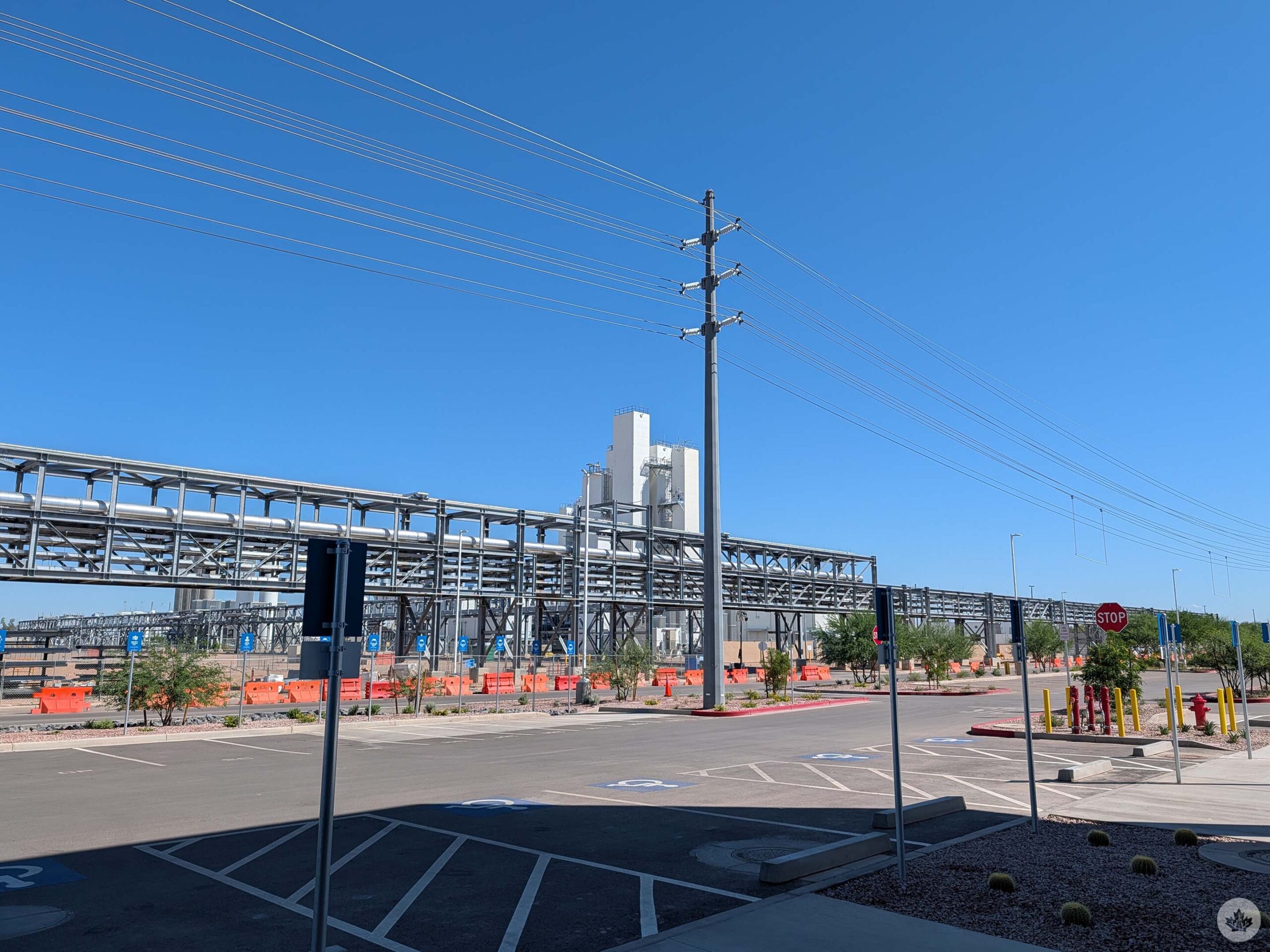
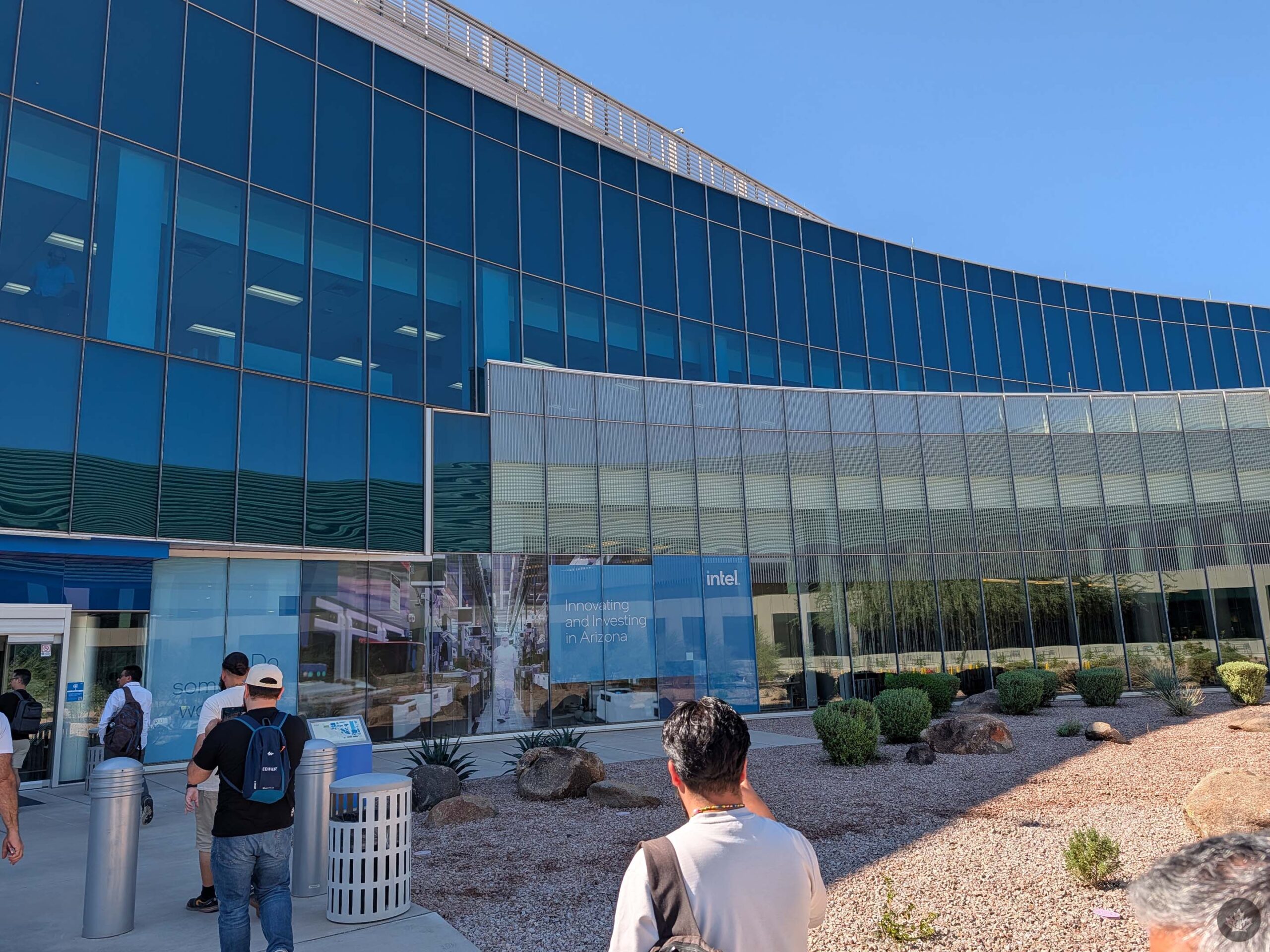
Old Price Road cuts sharply through the Arizona desert in its nearly straight north-south stretch. In the west, green fields give way to beige sand. Beyond them, the Sierra Estrella Mountains rise above a nearly flat landscape. On the other side of the road, a network of pipes connects a series of massive buildings, giving the whole thing a vaguely steampunk vibe. This is Intel's Ocotillo site in Chandler, Arizona, where some of the company's chipmaking facilities, called fabs, are located, including where the company produces new Panther Lake chips.
As part of my time at the Intel 2025 Tech Tour in Arizona earlier this month, I was able to visit the Ocotillo site and visit the new Fab 52 for an inside look at chip manufacturing. The tour began with a tour of the company's Arizona campus, which is just over one square mile and includes several manufacturing sites. All of the campus roads have chip-related names, such as Silicon Street, Processor Boulevard, and Transistor Terrace.
View of Sierra Estrella from the Intel Ocotillo campus.
There is also plenty of covered parking on campus – a boon in the summer when temperatures reach 45°C. But this is not only covering cars, but also solar panels. The energy Intel captures this way is returned to the city of Chandler.
This isn't Intel's only sustainability effort in Arizona. Another part of the campus we saw was the water treatment and recycling facilities and the Ocotillo Brine Reduction Facility (OBRF). OBRP removes salt from water before further purification, and the removed salt can be reused—Intel sells it to other companies.
A view of the water treatment system and piping at Intel's Ocotillo campus.
The 12-acre treatment facility, created through the Intel Chandler partnership, treats nine million gallons of water per day and returns it to the plant as a source of very clean water. Water is distributed throughout Ocotillo through a water distribution loop—some of the aforementioned pipelines around buildings. Factories use millions of gallons of water every day for a variety of tasksincluding cleaning silicon wafers used to make chips, for cooling, etc.
Moreover, Intel is committed to water resources in Arizona, conserving water through its operations while funding community water restoration projects. In 2023, these projects restored 1.1 billion gallons (4.16 billion liters) of water to the state.
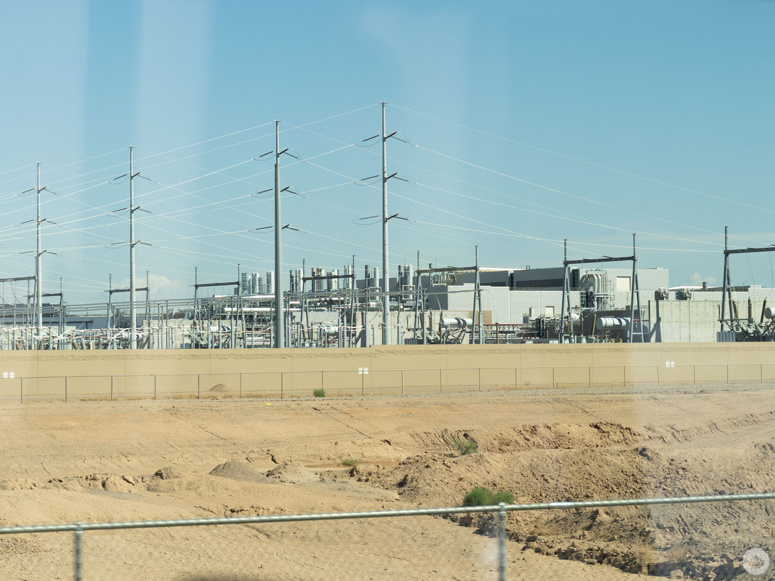
Electricity generation at the Ocotillo campus.
The Ocotillo campus also has its own power plant, providing approximately 100 megawatts of electricity to the area.
Change clothes to go inside
With the outside tour complete, we headed inside to see Fab 52. The scale of the facility was stunning, especially considering how small the final product is. Our guide noted that the entire factory is over a mile (1.6 km) long and the entire facility can be walked on foot.
But before we got inside, we needed to prepare. The Fab 52, like many other devices, needs to be kept incredibly clean, as even the smallest particles of dust can be catastrophic to the delicate circuitry of computer chips.
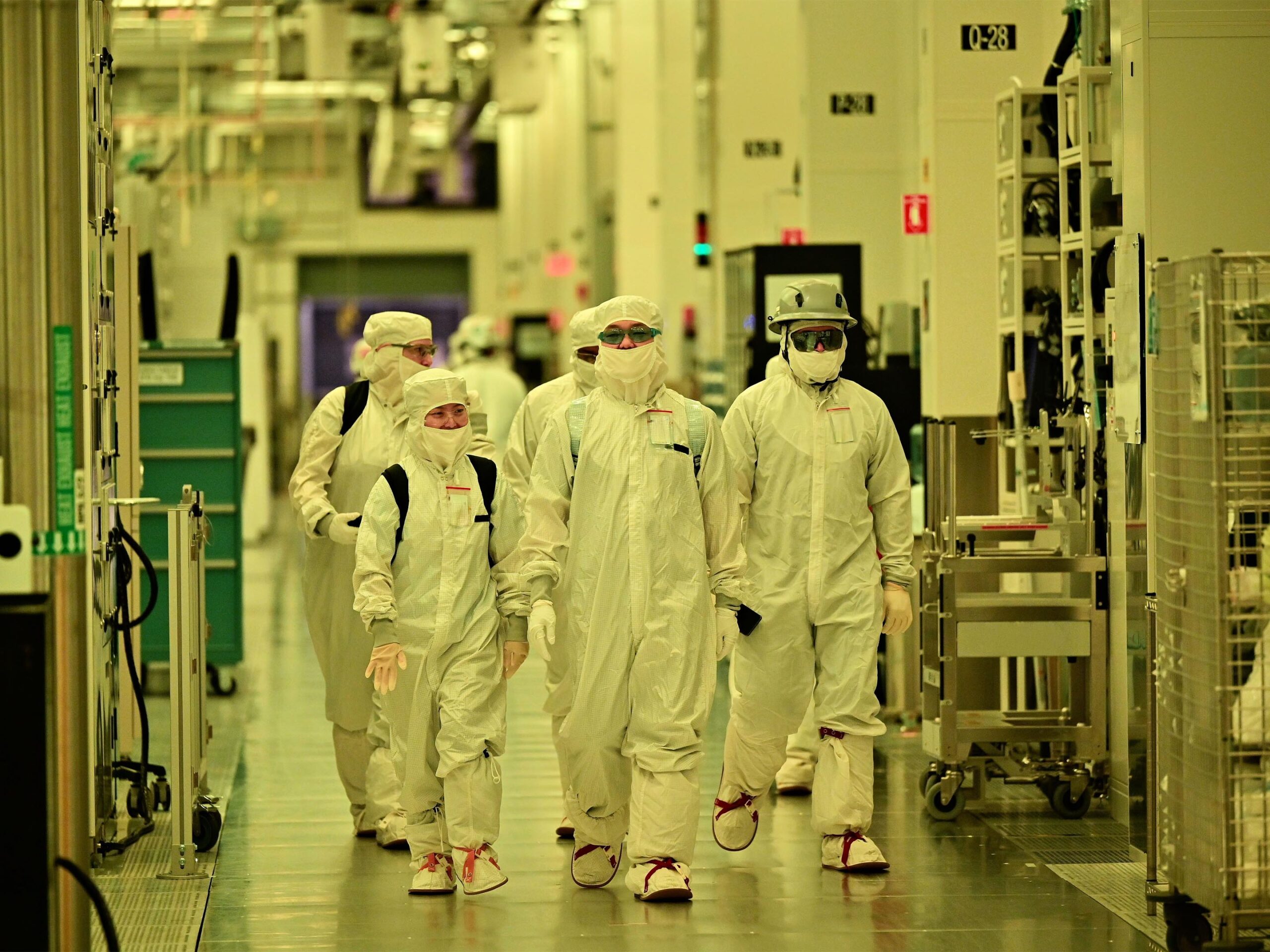
Intel workers in scrubs in the clean rooms of the plant. | Image credit: Intel.
Fab 52 is a Class 10 clean room, meaning it is approximately 100 times cleaner than an operating room, circulating air six times per minute. Moreover, the entire building is designed for a certain air movement: clean air is supplied through the ceiling, and the floor consists of perforated metal tiles that allow the air to escape.
But dust and dirt are not the only problems. We were unable to bring in any wireless devices such as phones or even smartwatches due to potential interference. Even copper was restricted: some workers in the factory wore pink suits to indicate that they could work with copper, to avoid contamination of non-copper areas. Intel also wouldn't allow us to import the cameras, mostly due to IP protection, since Intel also makes chips for other companies in its factory – while that's disappointing, the company provided plenty of photos of the inside of the Fab 52 that you'll see throughout this story.
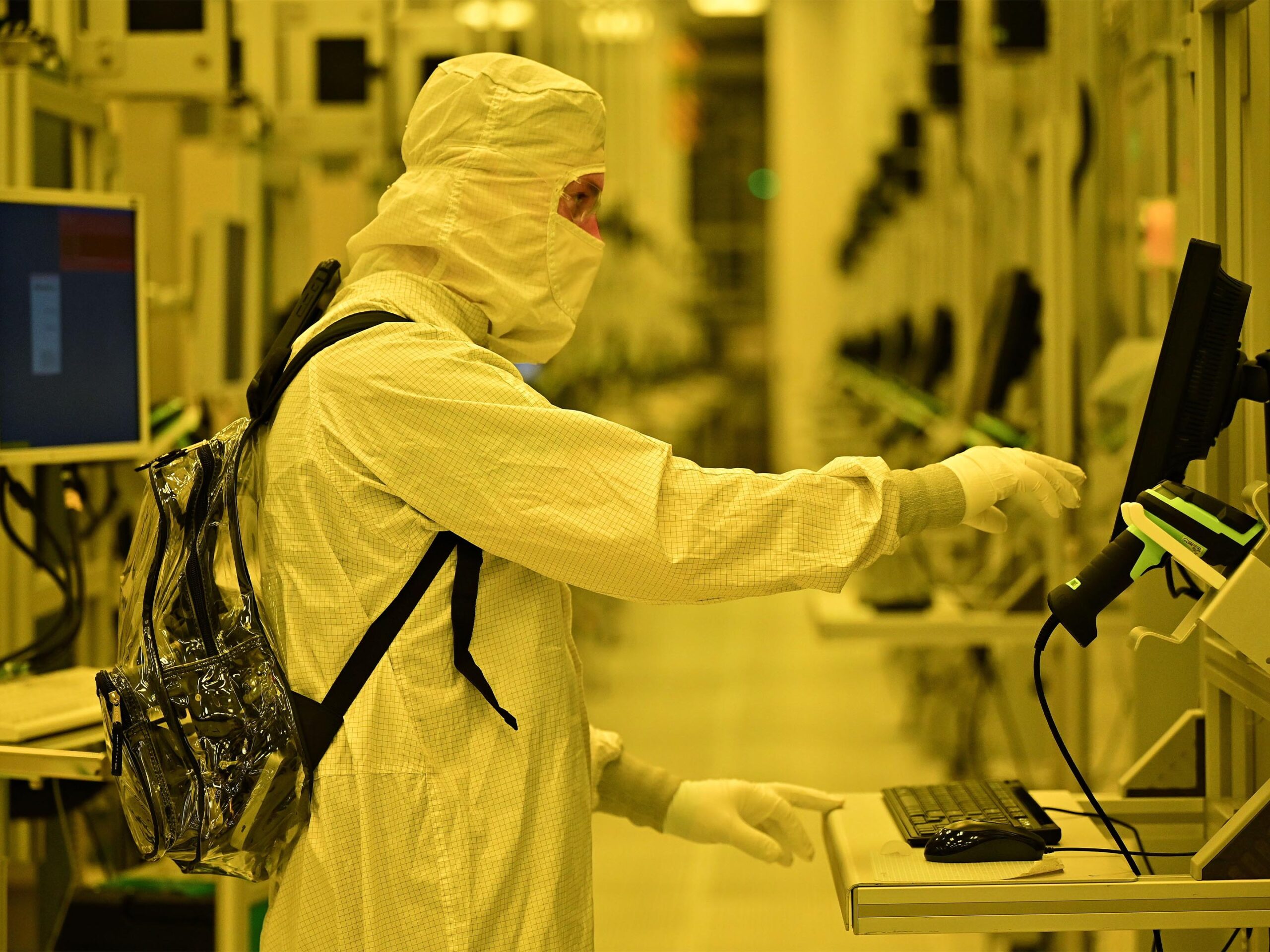
A worker performs tasks on a computer inside an Intel Fab 52. | Image credit: Intel.
With all our equipment safely stored, we headed towards the magnificent entrance. Entering the factory meant passing through a series of doors that resembled an airlock on a spaceship. Behind the doors was a dressing room where we all had to get dressed before entering the factory. Everyone entering must wear a hair and/or beard net, coveralls, hood, two pairs of boots, two pairs of gloves and safety glasses.
Once we were dressed, all that was left exposed was a narrow strip of our face, including our eyes and nose. The suits themselves weren't bulky and were actually very light, but were quite warm throughout. While we wore suits for no more than 30 minutes, those who work in factories wear them for hours and have to take them off and change every time they leave the factory, for example to go to the toilet or eat lunch. It took us a while to get through the dressing process, but for those who work in the factory, it's almost second nature and they can get dressed in less than five minutes.
Automated systems distribute silicon throughout the factory
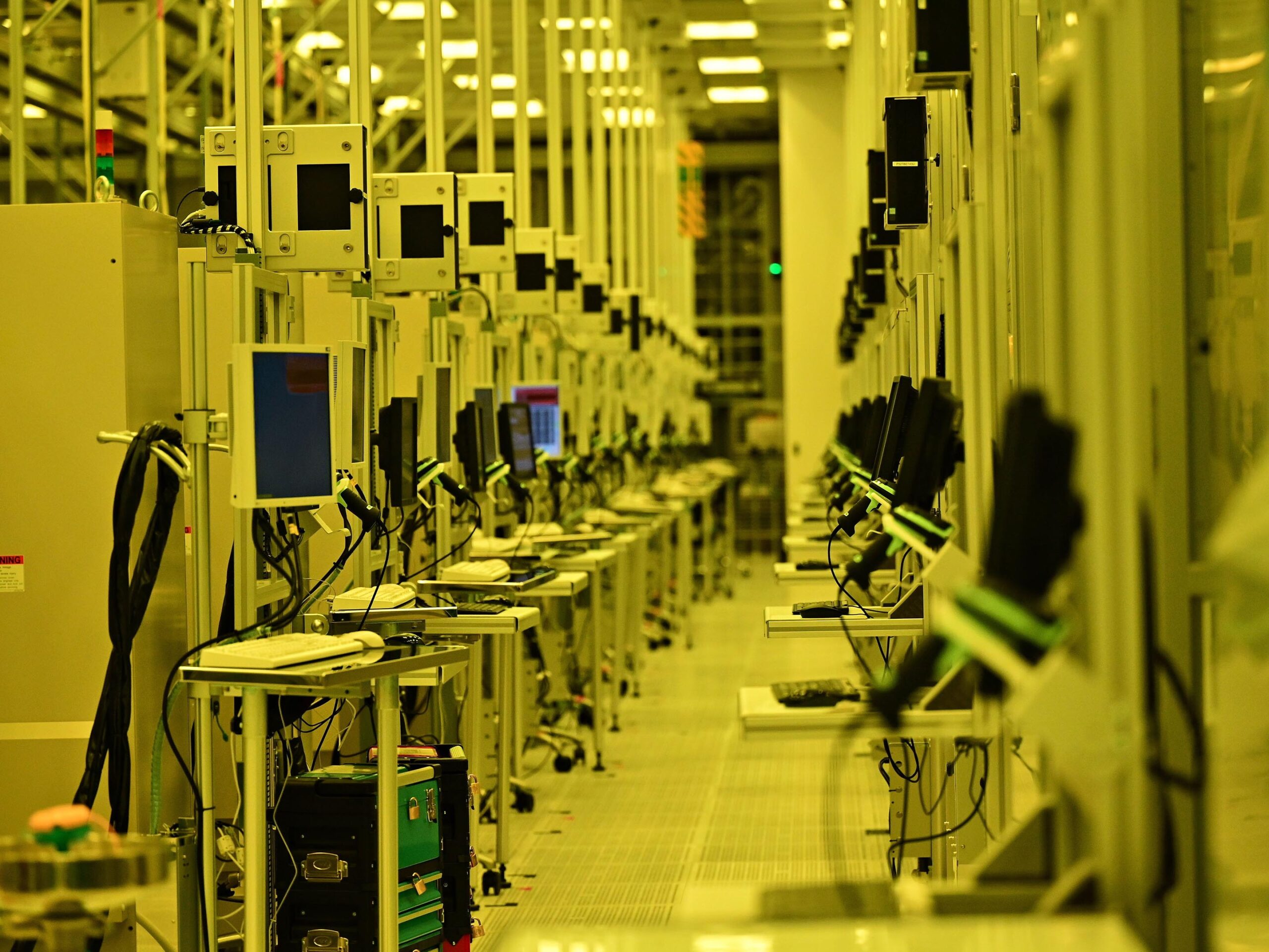
Equipment inside Fab 52. | Image credit: Intel.
Inside the factory, it was as if I had entered a completely different world, an advanced technological space of the future. The lighting was strangely yellow – and for good reason! — and everywhere I looked, cars were whirring, lights were flashing, and people in suits that looked like me were bustling about. Cars, barely larger than normal carry-on luggage, zipped overhead on the monorail system.
The overhead monorail is part of an automated materials handling system (AMHS) that uses overhead hoist conveyors (OHTs) with front-opening unitized containers (FOUPs) to transport materials such as silicon wafers throughout the factory. It was mesmerizing to watch the AMHS in action as the OHTs zipped along the tracks. At the junctions the OHTs looked like they were about to collide, but at the last second one slowed slightly to allow the other to pass safely before quickly picking up speed again.
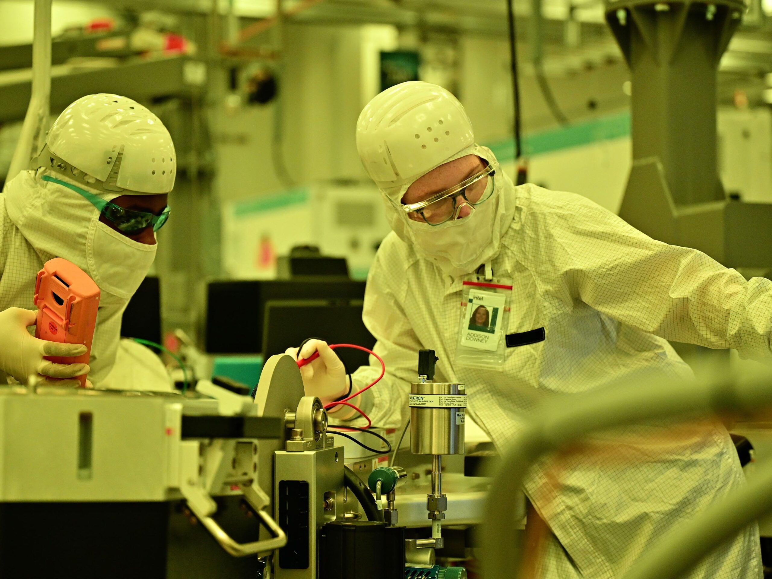
Image credit: Intel.
Intel Fab 52 has more than 30 miles (48.3 km) of AMHS to deliver wafers directly to parts of the plant, such as extreme ultraviolet (EUV) lithography machines. These machines are used to engrave patterns into silicon that form the inner workings of computer chips. The video below offers a decent basic explanation of the chip making process and even shows what OHT and FOUP look like.
These massive EUV machines can measure approximately 33 x 17 x 13 feet, weigh over 330,000 pounds and cost from 150 to 380 million US dollars. (from 210 to 533 million Canadian dollars). Intel said it will take 14 weeks from the time these tools arrive until they can begin production at the plant, and the company uses special sealed elevators to clean the components and transport them to a clean room. EUV machines are installed in sections with a special rigid structure to minimize vibrations, which can also negatively affect the etching process.
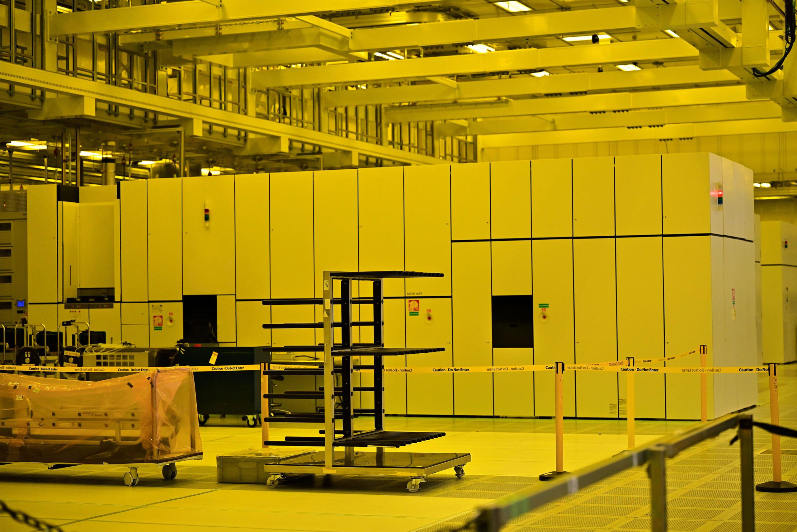
One of the EUV lithography machines inside a Fab 52. | Image credit: Intel.
As mentioned earlier, the factory's unusual yellow lighting is actually an important addition that both aids the lithography process and improves human vision. First, lithography uses a light-sensitive material called photoresist that responds to specific wavelengths of light. The yellow light used in factories has a wavelength that exceeds the sensitivity of the photoresist, meaning that exposure to light will not affect the lithography process.
Moreover, human eyes have better visibility with this type of lighting – Red lighting can make it difficult to recognize details, and green light can cause glare. Yellow lighting provides balance for better visibility without interfering with lithography and photoresist materials.
History of Intel in Arizona
An outside look at the Fab 52.
Intel first began operations in Arizona back in 1979 and has since invested US$50 billion (approximately C$70 billion) in its operations there, helping to transform the region into a major semiconductor manufacturing hub.
Intel's Arizona campus is just over one square mile in size and includes several manufacturing sites, including:
- Fab 12 opened in the 1990s and became one of Intel's most advanced manufacturing facilities.
- Fab 22, opened in 1996.
- Fab 32, built in the early 2000s.
- Fab 42, completed in 2017.
- Fab 52, laid down in 2021 and currently in service.
- Fab 62, part of an expansion that included Fab 52.
![]()
A typical US$20 to 25 billion (approximately C$28 to 35 billion CAD) factory takes three to five years to build. It's not hard to see why, given all the equipment and specialized tools required to produce chips. Again, it's hard to overstate the scale of the infrastructure used to create these tiny chips that power the devices we use every day.
Intel chips are used in laptops, desktops, and a variety of other electronics—and that's just Intel! There are several other chipmakers creating silicon for millions of devices, from smartphones to headphones and more. It's a little crazy how much goes into creating something that most people use on a daily basis without thinking about it.
MobileSyrup may earn a commission from purchases made through our links, which helps fund the journalism we provide for free on our website. These links do not influence our editorial content. Support us Here.


